
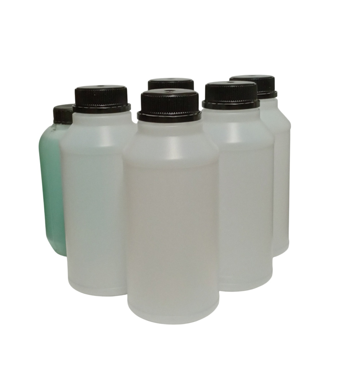
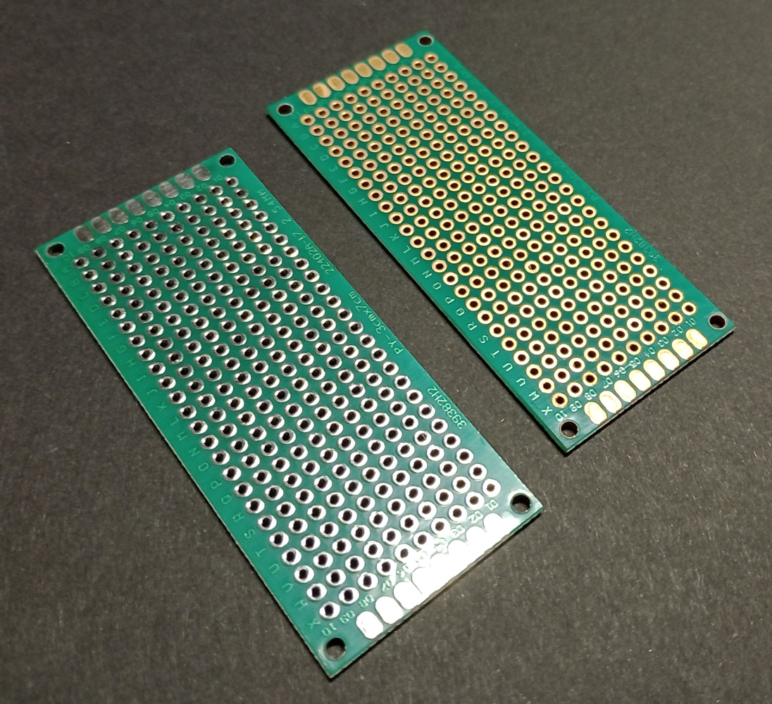
GRAFMETAL electroless gold plating of PCBs allows for effective gold plating of copper surfaces. This process is called ENIG process (electroless nickel, immersion gold). The kit contains solutions for surface preparation and electroless nickel solution, which is a substrate that should be used under the gold layer. With this kit one may carry out gold plating without utilizing electric current, which allows for gold plating of all the exposed copper parts, no matter what is the board topology. GRAFMETAL electroless gold plating allows for obtaining gold layers with a thickness of up to 0.2 μm (0.1 recommended) on nickel layer with a thickness of at least 1 μm (up to 4 μm). The kit contains 6 solutions with a volume of 1000 ml each:
Solution for alkaline degreasing
Solution for etching of copper
Solution for copper activation
Solution for deactivation
Electroless nickel plating solution
Electroless gold plating solution (2.5 g of potassium dicyanoaurate)
Each step is carried out in a following way:
Solution for alkaline degreasing, 1-10 min, room temperature
Rinsing in water
Rinsing in water
Solution for etching of copper, 1-30 min, room temperature
Rinsing in water
Rinsing in water
Solution for copper activation, 1 min, room temperature
Rinsing in water
Rinsing in water
Solution for deactivation, 1 min, room temperature
Rinsing in water
Rinsing in water
Electroless nickel plating solution, 7-30 min, 80°C, 1-4 μm Ni, avoid overheating
Rinsing in water
Rinsing in water
Electroless gold plating solution, 10 min, 85°C, 0.1 μm Au, gold plating speed will get slower over time
Rinsing in water
Rinsing in water
Rinsing water is not included in the kit, it is necessary to use demineralized water or distilled water or low hardness tap water. After each rinsing it is necessary to use another water, i.e. do not use one water container for many operations of rinsing. Water losses of nickel and gold plating solutions may be covered up by addition of water from rinsing right after those operations.
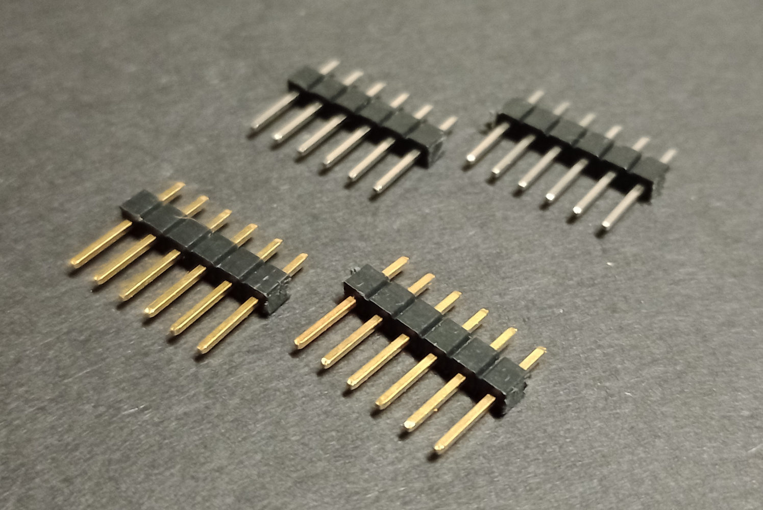
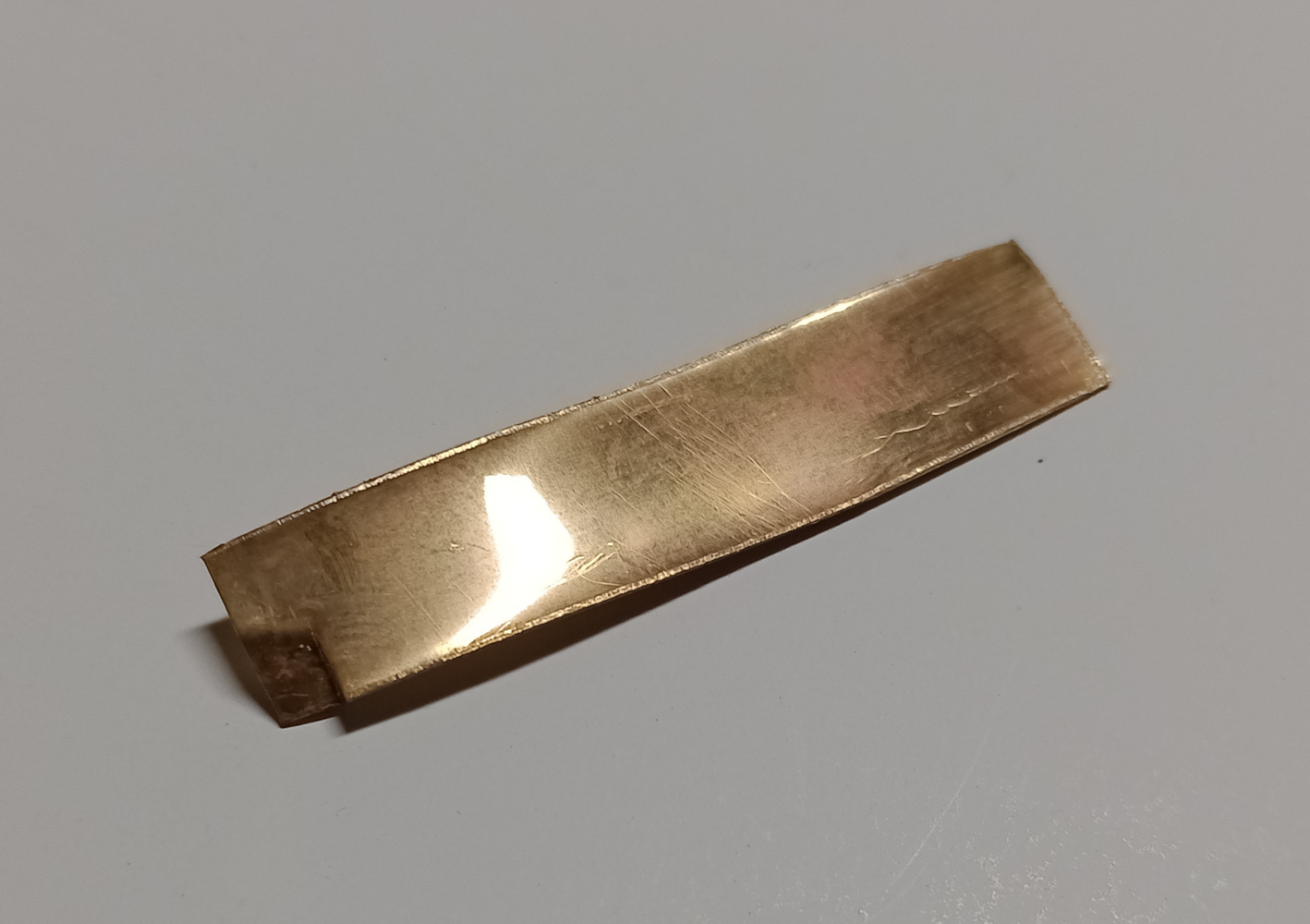
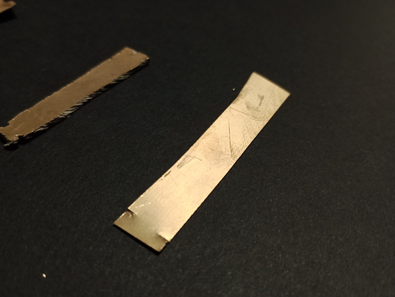
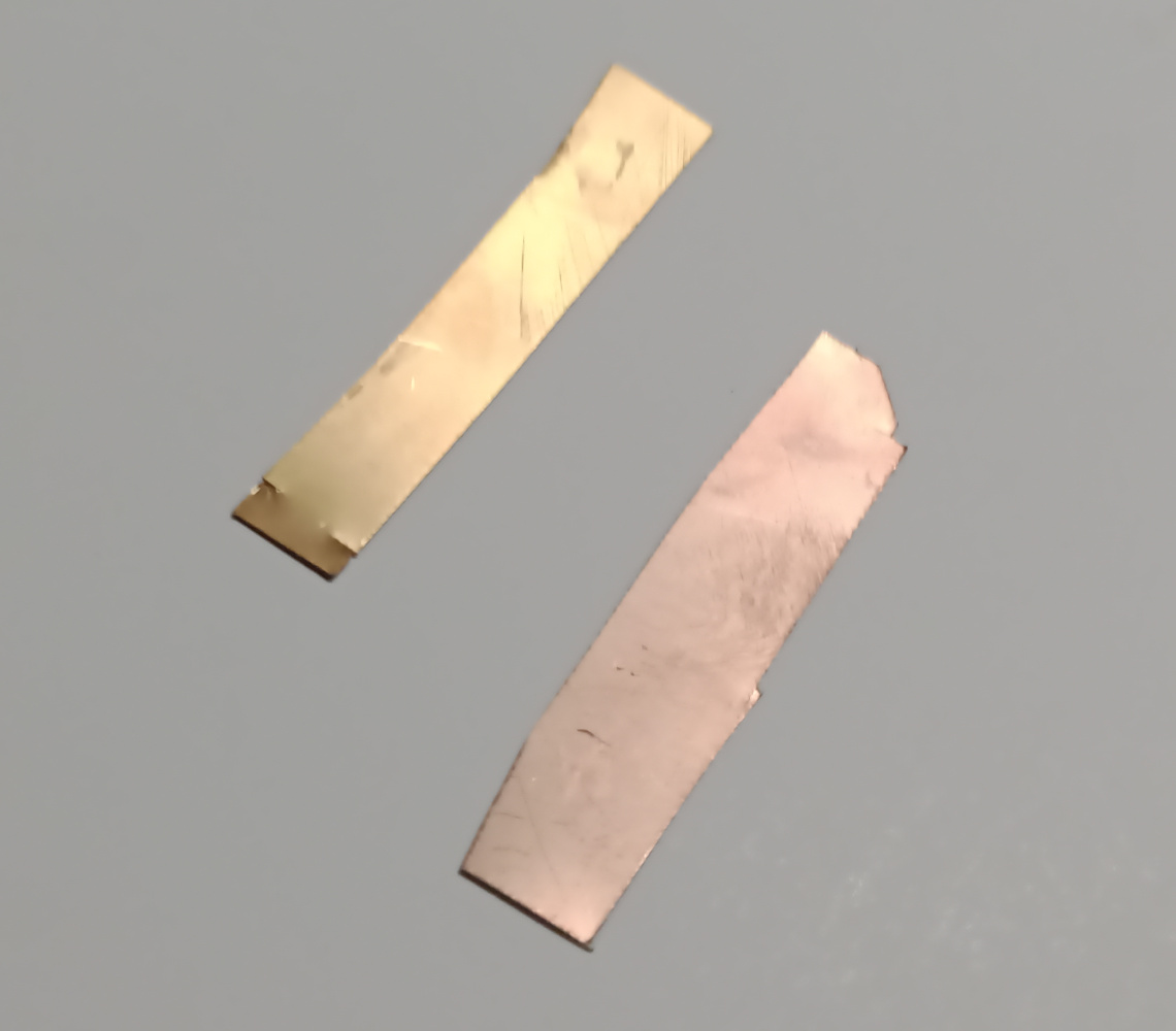
The best effects of gold plating are obtained on layers of electroless nickel, however it is noteworthy that satisfactory results were also noted for:
Copper
Ordinary steel (not for stainless steel)
Tin
Pure or electrolytic nickel
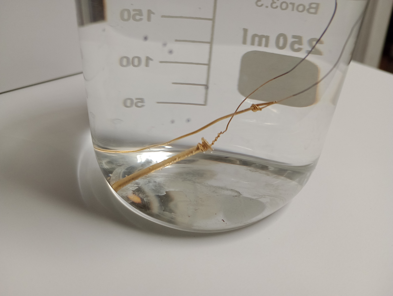
It is necessary to remember that gold and copper interdiffuse with each other at room temperature, so thin layers of gold on copper may exhibit limited lifetime and probably will not survive 10 years without oxidation.
If using proper etching solutions, it is possible to carry out electroless nickel plating and subsequent electroless gold even on stainless steel.
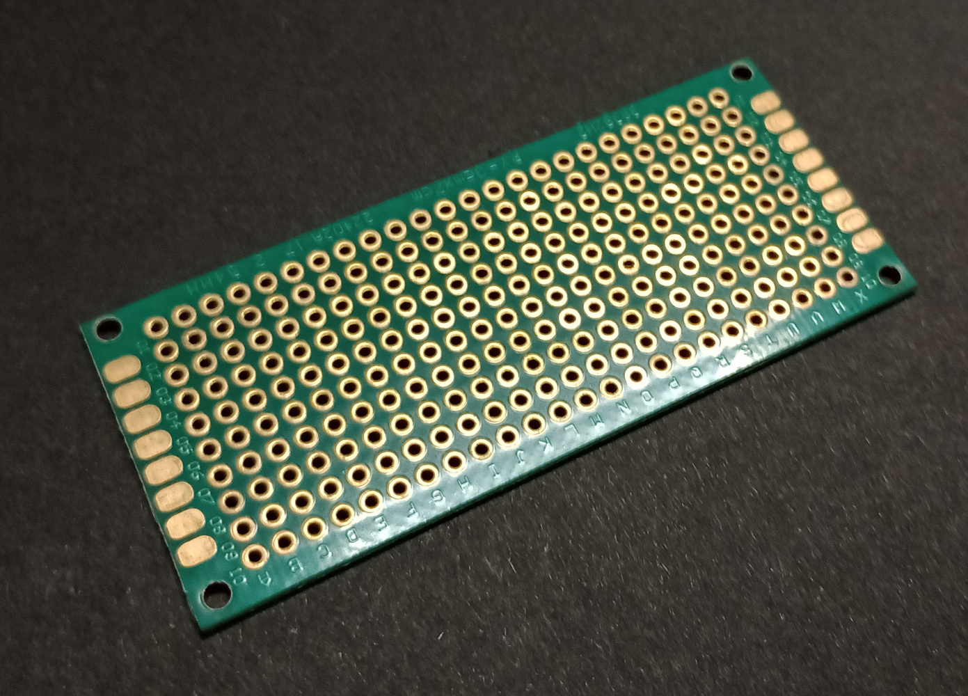
Thanks to using a special combination of 6 solutions, it is possible o plate PCB laminates, like FR4. As a result of nickel and gold plating, spaces between conductive paths are not coated with metal.
SERVICES. If you do not want to start gold plating in your facility, then we can offer a service of PCB gold plating on our own.